- 您现在的位置:买卖IC网 > Sheet目录3862 > PIC16F916-I/ML (Microchip Technology)IC PIC MCU FLASH 8KX14 28QFN
199
8018P–AVR–08/10
ATmega169P
20. USI – Universal Serial Interface
The Universal Serial Interface, or USI, provides the basic hardware resources needed for serial
communication. Combined with a minimum of control software, the USI allows significantly
higher transfer rates and uses less code space than solutions based on software only. Interrupts
are included to minimize the processor load. The main features of the USI are:
Two-wire Synchronous Data Transfer (Master or Slave)
Three-wire Synchronous Data Transfer (Master or Slave)
Data Received Interrupt
Wakeup from Idle Mode
In Two-wire Mode: Wake-up from All Sleep Modes, Including Power-down Mode
Two-wire Start Condition Detector with Interrupt Capability
20.1
Overview
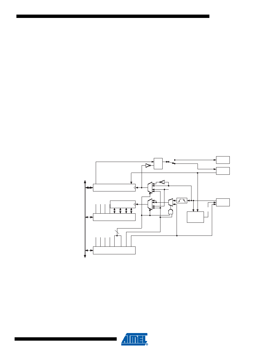
A simplified block diagram of the USI is shown on Figure 20-1. For the actual placement of I/O
pins, refer to Figure 1-1 on page 2. CPU accessible I/O Registers, including I/O bits and I/O pins,
are shown in bold. The device-specific I/O Register and bit locations are listed in the ”USI Regis-
Figure 20-1. Universal Serial Interface, Block Diagram
The 8-bit Shift Register is directly accessible via the data bus and contains the incoming and
outgoing data. The register has no buffering so the data must be read as quickly as possible to
ensure that no data is lost. The most significant bit is connected to one of two output pins
depending of the wire mode configuration. A transparent latch is inserted between the Serial
Register Output and output pin, which delays the change of data output to the opposite clock
edge of the data input sampling. The serial input is always sampled from the Data Input (DI) pin
independent of the configuration.
The 4-bit counter can be both read and written via the data bus, and can generate an overflow
interrupt. Both the Serial Register and the counter are clocked simultaneously by the same clock
source. This allows the counter to count the number of bits received or transmitted and generate
DATA
BUS
USIPF
USITC
USICLK
USICS0
USICS1
USIOIF
USIOIE
USIDC
USISIF
USIWM0
USIWM1
USISIE
Bit7
Two-wire Clock
Control Unit
DO
(Output only)
DI/SDA
(Input/Open Drain)
USCK/SCL
(Input/Open Drain)
4-bit Counter
USIDR
USISR
DQ
LE
USICR
CLOCK
HOLD
TIM0 COMP
Bit0
[1]
3
0
1
2
3
0
1
2
0
1
2
发布紧急采购,3分钟左右您将得到回复。
相关PDF资料
PIC16C716-20I/P
IC MCU OTP 2KX14 A/D PWM 18DIP
PIC18F26K80-I/SO
MCU PIC 64KB FLASH 28SOIC
PIC18F26J13-I/SS
IC PIC MCU 64KB FLASH 28SSOP
SFW27R-1STE1
SFW27R-1STE1-FFC/FPC CONN
PIC18F66J15-I/PT
IC PIC MCU FLASH 48KX16 64TQFP
PIC24FV32KA302-I/SO
MCU 32KB FLASH 2KB RAM 28-SOIC
PIC24HJ64GP204-I/ML
IC PIC MCU FLASH 64K 44-QFN
SFW27R-2STE1
SFW27R-2STE1-FFC/FPC CONN
相关代理商/技术参数
PIC16F916-I/SO
功能描述:8位微控制器 -MCU 14KB FL 352R 25 I/O RoHS:否 制造商:Silicon Labs 核心:8051 处理器系列:C8051F39x 数据总线宽度:8 bit 最大时钟频率:50 MHz 程序存储器大小:16 KB 数据 RAM 大小:1 KB 片上 ADC:Yes 工作电源电压:1.8 V to 3.6 V 工作温度范围:- 40 C to + 105 C 封装 / 箱体:QFN-20 安装风格:SMD/SMT
PIC16F916-I/SO
制造商:Microchip Technology Inc 功能描述:8 Bit Microcontroller Clock Speed:20MHz
PIC16F916-I/SOG
制造商:Microchip Technology Inc 功能描述:8BIT MCU FLASH SMD 16F916 SOIC28
PIC16F916-I/SP
功能描述:8位微控制器 -MCU 14KB FL 352R 25 I/O RoHS:否 制造商:Silicon Labs 核心:8051 处理器系列:C8051F39x 数据总线宽度:8 bit 最大时钟频率:50 MHz 程序存储器大小:16 KB 数据 RAM 大小:1 KB 片上 ADC:Yes 工作电源电压:1.8 V to 3.6 V 工作温度范围:- 40 C to + 105 C 封装 / 箱体:QFN-20 安装风格:SMD/SMT
PIC16F916-I/SP
制造商:Microchip Technology Inc 功能描述:8 Bit Microcontroller Clock Speed:20MHz
PIC16F916-I/SS
功能描述:8位微控制器 -MCU 14KB FL 352R 25 I/O RoHS:否 制造商:Silicon Labs 核心:8051 处理器系列:C8051F39x 数据总线宽度:8 bit 最大时钟频率:50 MHz 程序存储器大小:16 KB 数据 RAM 大小:1 KB 片上 ADC:Yes 工作电源电压:1.8 V to 3.6 V 工作温度范围:- 40 C to + 105 C 封装 / 箱体:QFN-20 安装风格:SMD/SMT
PIC16F916-I/SS
制造商:Microchip Technology Inc 功能描述:8-Bit Microcontroller IC
PIC16F916T-E/MLC02
制造商:Microchip Technology Inc 功能描述: